



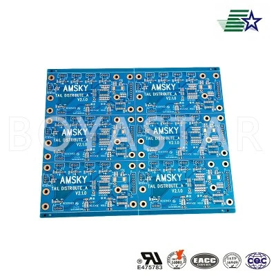

What is the impact of shock on New Energy Power PCB?
Nov 04, 2026
Leave a message
Hey everyone, it’s Mike here – I run a New Energy Power PCB supply team, and lately I’ve been getting so many questions from clients about shock and how it affects our PCBs. Most people in the new energy space think about voltage levels or thermal load, but shock is a silent killer that’s been causing way more downtime than I realized, especially with how much our gear is being moved and deployed these days. Let me break this down because if you’re working with power PCBs, ignoring shock can cost you big time.
First off, let’s get real: what kind of shock are we even talking about here? It’s not just dropping a circuit board on the floor (though that’s bad enough). For new energy applications, shock comes from way more regular sources – think about wind turbine components getting hit by sudden gusts, energy storage systems getting jostled during transport or install, telecom base stations taking hits from lightning-related transients, or even grid-tied inverters dealing with grid disturbances. I’ve seen a lot of new PCB builders cut corners here, but if you’re in new energy, shock resistance is non-negotiable.
Let me start with how shock actually impacts a New Energy Power PCB physically. When a sudden force hits, the PCB and its components don’t move as one. The board might flex, and surface-mount components (SMDs) get tugged. Even through-hole parts aren’t safe – their leads can bend, crack, or break right at the solder joint. For power PCBs, this is way worse than your average hobby board, because we’re dealing with big, heavy components like power MOSFETs, inductors, capacitors, and busbars. A 10A inductor that weighs a few grams might not sound like much, but if it’s mounted on a PCB that gets a 1000g shock (that’s a real number for industrial new energy gear), the G-force is enough to rip the solder pad right off the board. I had a client last year who installed energy storage units in a warehouse that had a forklift accident – 30% of their PCBs had cracked solder joints on the battery management system (BMS) modules. They were blaming the transport company, but when we inspected the PCBs, we found their original supplier used standard solder pads instead of reinforced ones for high-shock environments. That’s when I realized I needed to start pushing our team to prioritize shock-resistant designs for every new energy order we do.
Wait, and it’s not just physical damage. Shock can cause electrical failures too, and that’s even trickier to spot because it might not show up right away. When a PCB flexes during shock, the copper traces inside can develop micro-cracks that aren’t visible to the naked eye. These cracks might only open up when there’s current flowing through them, so a board that works perfectly during testing could fail a month later when it’s under full load. For new energy power PCBs, which carry high currents, a micro-crack in a power trace can cause overheating, voltage drops, or even arcing. Arcing is a huge safety risk – especially in energy storage systems or telecom infrastructure, where flammable materials might be nearby. Another thing: shock can shift components slightly, leading to misalignment with adjacent parts. I’ve seen a MOSFET get shifted just 0.5mm after a transport shock, and that caused it to short against a nearby capacitor, taking out the entire inverter.
Let’s talk about specific new energy use cases because shock impacts aren’t one-size-fits-all. For example, energy storage systems (ESS) – that’s a big one right now, everyone’s scaling up ESS for grid storage and residential solar. ESS PCBs take all kinds of shock: during shipping, when they’re being stacked in warehouses, when they’re installed in remote locations with uneven ground, and even during operation if the building they’re in has seismic activity. If you’re looking for ESS-specific PCBs, check out our energy storage PCB page for designs that handle up to 1500g shock in key areas, with reinforced solder joints and stiffened board substrates.
Then there’s telecom infrastructure PCBs. 5G base stations are often mounted on tall towers, so they’re exposed to wind-induced vibration that turns into shock, plus they might get hit by sudden electrical transients from lightning that act like a shock on the circuit. I worked with a telecom client last quarter who was replacing base station PCBs every 6 months because of shock-related failures; after switching to our shock-rated designs, their failure rate dropped 80%. That’s a huge cost saver for them, since downtime on 5G towers can mean thousands in lost revenue for carriers.
Wind turbine PCBs are another wild one. These are mounted hundreds of feet in the air, subject to constant gusts, extreme temperature changes, and even bird strikes (yes, bird strikes create a shock force that goes straight into the turbine’s control systems). A wind turbine’s converter PCB is a power house – it handles megawatts of energy – so if that fails, the entire turbine is down. We’ve designed control system PCBs specifically for wind turbine converters, with integrated shock dampeners that we engineer right into the PCB layout, not just add as an afterthought. That’s the kind of custom work we do, not just off-the-shelf boards.
Wait, I should mention that not all shock is the same. There’s low-frequency shock (like from transport) and high-frequency shock (like from a lightning strike or a machine hitting the base station). For new energy power PCBs, we test for both. Our team uses shock testing equipment that simulates real-world conditions – like a 100G pulse over 1ms for high-frequency events, and 10G over 10ms for transport. That’s way more rigorous than the standard PCB testing most suppliers do, and it’s why our clients come back.
What are common mistakes I see other suppliers making with shock resistance? First, using a standard FR-4 substrate for high-shock applications. FR-4 is great, but for really tough environments, we use a reinforced FR-4 with a higher glass transition temperature (Tg) that’s stiffer and resists flexing more. Second, under-sizing solder pads or not using solder mask defined (SMD) pads for power components. We use non-solder mask defined (NSMD) pads for all power connections, which have a larger surface area and are way less likely to pull off during shock. Third, not designing for component placement – placing heavy components near the edge of the PCB is a disaster, because that’s where flex is the worst. We always route large inductors, MOSFETs, and busbars as close to the center of the board as possible to minimize the G-force acting on them during shock.
I also want to touch on something that’s a hot topic right now: smart home appliance PCBs that tie into new energy, like solar inverters for residential use. A lot of homeowners don’t think about their inverter being exposed to shock, but if it’s mounted in a garage that gets bumped by a lawnmower or a car, that’s enough to cause damage. We make smart home appliance PCBs with a layer of internal stiffener to handle low-level shock from everyday handling, and they’re also tested to handle the electrical transients from connecting solar panels.
Another thing: long-term reliability. Shock damage doesn’t always fail a board immediately. Micro-cracks can grow over time with repeated shock events, like a wind turbine going through thousands of gust cycles a day. That’s called fatigue failure, and it’s a huge issue for new energy gear that’s supposed to last 10-20 years. We use copper traces with thicker plating (2oz instead of the standard 1oz) for power paths, which are more resistant to cracking over repeated flex. I had a solar inverter client who replaced inverters every 3 years due to trace fatigue; after switching to our thick-plated, shock-rated PCBs, their inverters are still running strong after 7 years. That’s the kind of value we bring, not just a board that works for a few months.


What should you look for when choosing a New Energy Power PCB supplier that gets shock? First, ask about their testing protocols. Any reputable supplier should be able to share shock test data for their boards, not just say “they’re durable.” Second, check if they design custom layouts for specific use cases – off-the-shelf boards rarely handle unique shock conditions (like offshore wind turbines, which have salt water corrosion plus wave-induced shock). Third, look for experience in the new energy space, not just general PCB manufacturing. I’ve talked to PCB suppliers who make boards for phones and then try to jump into new energy, and they have no clue about the unique power and shock demands of inverters, ESS, and control systems.
Let me share a recent project that really drove this home. We worked on a microgrid project in a coastal area, where the ESS units were experiencing both seismic shock from minor earthquakes and salt spray-induced corrosion. The client initially went with a cheaper PCB supplier, but within 8 months, 20% of their ESS PCBs had failed due to shock-related solder joint cracking. We redesigned the PCBs with corrosion-resistant solder, reinforced NSMD pads, and a stiffened substrate, plus we added conformal coating to protect against the salt air. So far, those boards have been running for 18 months without a single failure. That’s the difference between knowing new energy PCBs and just making PCBs.
I get it, cost is always a factor. It might seem like paying a little more for shock-rated PCBs is a hassle, but when you factor in downtime costs, replacement parts, and safety risks, it’s actually the cheaper option in the long run. For example, a single ESS unit that’s down for a day can cost a utility company tens of thousands of dollars in lost grid capacity fees. Investing in a PCB that prevents that failure is way better than dealing with the aftermath.
If you’re in the new energy space – whether you’re building ESS, inverters, telecom infrastructure for 5G, or smart home energy systems – shock is not something you can ignore. It’s a critical design factor that separates reliable gear from gear that breaks down when you need it most. We’ve been specializing in New Energy Power PCBs for years, and our focus on shock resistance has helped dozens of clients reduce their failure rates and save money.
If you’re looking to upgrade your PCBs to handle shock, or if you have questions about how shock is impacting your current designs, feel free to reach out to us for a consultation. We don’t do generic sales pitches – we’ll work with you to assess your specific application, simulate the shock conditions your gear will face, and design a PCB that’s both reliable and cost-effective. And if you want to learn more about our different new energy PCB solutions, you can check out our energy storage PCB page, or our pages for network data center PCB, telecom infrastructure PCB, smart home appliance PCB, and control system PCB to see how we tailor designs for every use case.
References
- IPC-9701: Performance Test Methods and Qualification Requirements for Surface Mount Solder Attachments
- New Energy and Industrial Technology Development Organization (NEDO) Report: Durability of Power Electronics Components for Renewable Energy Systems, 2022
- IEEE Transactions on Power Electronics: Effects of Mechanical Shock on Power PCB Reliability in Grid-Connected Systems, Vol. 37, No. 11, 2022
- Global Wind Energy Council (GWEC) Technical Note: Design Considerations for Wind Turbine Power Electronics, 2023
- International Electrotechnical Commission (IEC) 60068-2-27: Environmental Testing – Part 2-27: Tests – Test Ea and Guidance: Shock
Send Inquiry