





How to optimize the production process of hard gold plated PCB?
Nov 02, 2026
Leave a message
If you’ve ever worked with electronics manufacturing, you know that the performance of a final product often hinges on the smallest components—and that’s especially true when it comes to printed circuit boards (PCBs) requiring gold plating. As a Hard Gold Plated PCB supplier, I’ve spent years refining our production processes to balance durability, conductivity, and cost without cutting corners. Over time, I’ve learned that optimizing hard gold plating isn’t just about following a standard set of steps—it’s about understanding every variable that impacts the final result, from material selection to quality control. In this post, I’ll break down the actionable strategies we use to streamline our production, reduce waste, and deliver consistent, high-quality boards that meet even the most demanding client needs.
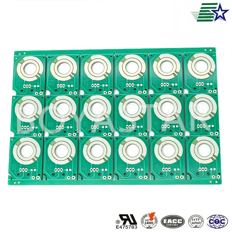
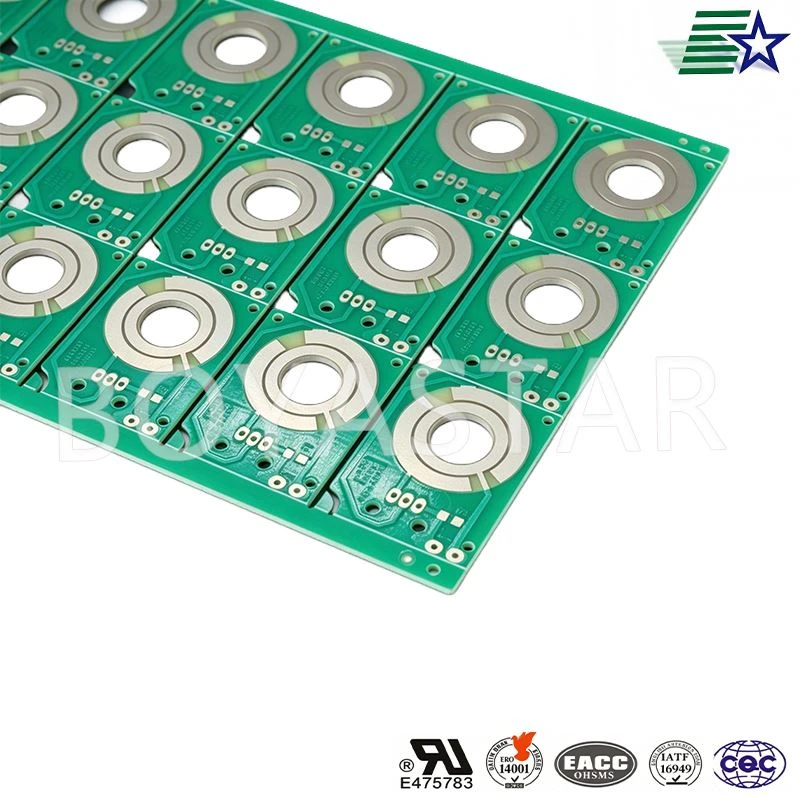
First, let’s get clear on what makes hard gold plating different from other surface finishes, because that’s the foundation of any optimization effort. Unlike soft gold, which is often used for wire bonding, hard gold is alloyed with elements like cobalt, nickel, or iron to create a wear-resistant surface perfect for connectors, gold fingers, and boards that will face repeated mating cycles. That durability makes Hard Gold Plated PCB a go-to for industries like aerospace, automotive, and medical devices, where failure isn’t an option. But that same hardness introduces unique challenges during production—things like controlling deposit thickness, avoiding porosity, and ensuring adhesion to the underlying base metal. If you’re new to surface finishes, comparing hard gold to other options can help you frame priorities: for example, OSP PCB is a simpler, more cost-effective finish for low-wear applications, while ENIG PCB offers excellent flatness for surface mount technology. Even ENEPIG PCB, a newer hybrid finish, combines multiple layers for extra protection, but it doesn’t replace hard gold in high-wear scenarios.
The first big optimization we made was overhauling our pre-treatment process, and it’s been a game-changer. Pre-treatment is often an afterthought for many shops, but we’ve found that 60-70% of plating defects come from poor surface preparation. When copper boards come out of their etching and cleaning steps, they have micro-oxidation and residual contaminants that make it impossible for gold to adhere evenly. Our old pre-treatment line was a series of tanks with generic acid cleaners and micro-etchers, but we noticed inconsistent results on boards with fine-pitch patterns, where even a tiny spot of poor adhesion would cause a whole batch to fail. We switched to a two-step pre-treatment specifically formulated for hard gold plating: first, a permanganate clean to strip any organic residues, followed by a mild acid dip and a soft micro-etch to create a uniform, slightly rough copper surface without over-erosion. We also added in-line conductivity testing after pre-treatment, so any boards that don’t meet our minimum copper surface resistance get routed back for reprocessing before they ever hit the plating line. This small change cut our adhesion-related defects by 45% within three months, which translated to less rework and faster turnaround for clients.
Next, we focused on optimizing the gold plating bath and deposition parameters—this is where the actual hard gold layer is applied, and even small adjustments here have huge impacts. For years, we used a standard hard gold bath with fixed concentrations of our cobalt alloy, but we noticed that batches produced during high humidity months had slightly higher porosity. After working with our chemical supplier, we learned that humidity affects the concentration of free cyanide in the bath, which in turn impacts how evenly the gold deposits. We now monitor both bath temperature (we keep it strictly at 55°C ± 1°C) and cyanide levels in real time with inline sensors, and we adjust our alloy concentration by 0.5 g/L based on daily humidity readings. We also replaced our old rack plating system with a new selective rack setup that holds boards securely without touching the plating surface, eliminating the need for tape or masking that can leave residual adhesive. For boards with gold fingers, we specifically program the rack to leave only the finger area exposed, reducing over-plating on non-critical areas and cutting down on post-plating polishing time. We also run periodic Hull Cell tests every two weeks to verify that the gold deposit is uniform across voltage levels—this helps us catch issues with anode wear or bath contamination before they affect production.
One of the most underrated areas of optimization is waste reduction and material reuse, which not only lowers costs but also aligns with our commitment to sustainable manufacturing. Hard gold is a precious metal, so even small amounts of excess plating add up quickly. Our old process used a dedicated dump tank for rinse water after plating, which had gold concentrations high enough that we were sending hundreds of liters of gold-contaminated water to treatment every month. We installed a counter-current rinse system: the final rinse uses water from the last rinse tank, which is in turn filled from the previous tank, and so on, back to the pre-plate rinse. This cuts water usage by 70% and reduces gold loss because the final rinse water has a high enough gold concentration that we can send it back to our gold recovery unit instead of treating it as waste. We also implemented a bath filtration schedule that uses 5-micron filter pads every 48 hours, instead of the weekly schedule we used before. Removing particulates from the bath prevents them from getting trapped in the gold layer, which causes roughness and wear issues—this has reduced our average gold layer thickness from 0.8 microns to 0.5 microns without sacrificing durability, saving us approximately 12 kg of gold per year. That’s not just a cost win; it’s also a better outcome for our clients, since thinner, uniform gold layers can still meet IPC standards while reducing overall material costs.
Quality control (QC) is the final piece of the optimization puzzle, and we’ve built it into every step of production instead of leaving it as a final inspection. For hard gold plating, IPC-4552 is the standard that defines thickness, porosity, and wear resistance requirements, so we’ve aligned our QC processes around that. We used to do a single gold thickness test per batch, taking a measurement from the edge of the board, but fine-pitch PCBs often have uneven thickness across the board surface. We now use X-ray fluorescence (XRF) scanners that test 5 random points per board, including the center and edges, and we log all data in a cloud-based system that our engineers can access in real time. We also added a wear resistance test: after plating, small sample coupons from each batch are subjected to a rubbing test to simulate mating cycles, and we check for gold transfer to the rubbing pad. This test catches defects that thickness testing alone would miss. For gold finger boards, we also do a contact resistance test after plating, since high contact resistance is a common failure point for connectors. If a batch fails any test, we don’t just rework the bad boards—we trace the issue back to its root cause, whether that’s a worn anode or a contaminated pre-treatment tank, so we can prevent the same problem from happening again.
Another key optimization has been integrating our production planning with client specifications, which has reduced lead times and minimized rework. Many clients come to us with specific requirements for Hard Gold Plated PCB that go beyond basic thickness—like porosity levels for high-frequency applications, or specific alloy ratios for medical devices. We used to have to reconfigure plating parameters manually for each new client, but we’ve built a database of standard parameters for common specifications, and our ERP system automatically pulls the right settings when a new order is placed. For example, if an order is marked for aerospace use, the system sets a higher micro-etch level in pre-treatment and adjusts the gold bath pH to ensure lower porosity. This has reduced order setup time by 30% and has cut down on errors from manual parameter selection. We also work with clients early in the design process to recommend material choices that are compatible with hard gold plating—for example, if a client is considering OSP PCB for a low-wear section but needs gold plating for connectors, we can suggest a combination of finishes that works best, instead of making them redesign later.
Looking back at the past five years of refining our process, the biggest lesson I’ve learned is that optimization isn’t a one-time project—it’s an ongoing cycle of testing, adjusting, and learning. Every time we make a small change, whether it’s a new pre-treatment chemical or a QC test, we track the impact closely, because what works for one type of board (like a gold finger PCB) might not work for a high-frequency board with fine lines. As a supplier, our goal isn’t just to produce PCBs that meet standards—it’s to deliver solutions that help our clients succeed, which means our production processes have to be flexible, consistent, and efficient. If you’re looking for a partner that understands the nuances of hard gold plating, from pre-treatment to final testing, we’re here to help you navigate every step. Contact our team today to discuss your Hard Gold Plated PCB needs, or learn more about our surface finish capabilities for other applications, including ENIG PCB, ENEPIG PCB, and OSP PCB.
References
IPC Association. (2020). IPC-4552: Performance Specification for Plated Coatings of Gold and Gold Alloys for Electronic Applications.
Schlesinger, M. (2010). The Gold Plating Handbook: Principles, Processes, and Practice. Elsevier.
Groover, M. P. (2019). Fundamentals of Modern Manufacturing: Materials, Processes, and Systems (7th ed.). Wiley.
Brown, J. R. (2018). Surface Finish Technology for Printed Circuit Boards. CRC Press.
Send Inquiry