



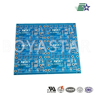

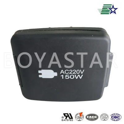
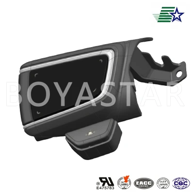


Communication Equipment PCB
The Communication Equipment PCB service is built for base stations and transmission equipment. High frequency and low loss are the core requirements. Our factory has 137 machines. These machines cover drilling, lamination, plating, etching, solder mask, silkscreen, AOI, and flying probe testing. The plant covers 19,000 square meters. We have more than 150 employees. We produce about 50,000 square meters of PCB each month.
Send Inquiry
High Frequency and Low Loss
The Communication Equipment PCB service is built for base stations and transmission equipment. High frequency and low loss are the core requirements. Our factory has 137 machines. These machines cover drilling, lamination, plating, etching, solder mask, silkscreen, AOI, and flying probe testing. The plant covers 19,000 square meters. We have more than 150 employees. We produce about 50,000 square meters of PCB each month. This board fits base station equipment, microwave transmission equipment, optical communication modules, satellite communication terminals, signal repeaters, and indoor distribution systems. Communication power supplies and communication antennas also use it. We use FR-4 as the base material. High TG FR-4 is also available. We support 4 to 20 layers with high-frequency signal transmission and low-loss design. High-frequency boards, low-loss boards, and high-reliability boards are all within our experience.

Impedance and Material Support
High CTI FR-4 is optional. Thick copper, impedance control, blind and buried vias, and BGA are all available. Immersion gold, HASL, and OSP are common options. Immersion silver, immersion tin, and hard gold plating are also available. Our engineering team has more than ten engineers. They do high-frequency signal review and impedance calculation. They send a formal quote and lead time within one day. We accept OEM and ODM orders. We build from drawings or samples. Layer count, stack-up, board thickness, copper thickness, base material, surface finish, solder mask color, silkscreen color, impedance, blind and buried vias, BGA, and packing are all customizable. The dielectric loss of high-frequency boards directly affects insertion loss. We recommend suitable base materials based on the buyer's frequency band. This keeps signal attenuation low during transmission. Base station equipment runs outdoors all year. The board must resist moisture and temperature changes. Our process control meets these requirements.

Signal Tests and Full Records
Signal loss is the top risk for communication boards. We run impedance tests, signal integrity tests, and insertion loss tests. We confirm the first article before release. We keep records for every step from incoming material to final shipment. Our quality team has more than 20 people. Every board gets 100% electrical testing before packing. We use AOI and flying probe testing. We accept third-party inspection. Our factory holds IATF16949, ISO9001, ISO14001, and ISO45001. We hold Underwriters Laboratories product safety certification. The file number is E528398. These approvals help us serve North American customers. The Communication Equipment PCB service gives buyers a reliable path for high-frequency designs.

Specifications Buyers Need to Know
|
Parameter |
Content |
|
Product Type |
Communication equipment PCB for base stations, microwave transmission, optical communication, satellite communication, signal repeaters |
|
Base Material and Layers |
FR-4, high TG FR-4, high CTI FR-4; supports 4 to 20 layers |
|
Key Processes |
High-frequency signal transmission, low-loss design, impedance control, blind and buried vias, BGA |
|
Surface Finish |
Immersion gold, HASL, OSP, immersion silver, immersion tin, hard gold plating optional |
|
Engineering Support |
High-frequency signal review and impedance calculation |
Hot Tags: communication equipment pcb, China communication equipment pcb manufacturers, suppliers, factory
Previous:Instrumentation PCB
Next:No Information
You Might Also Like


Send Inquiry