




Gold Finger PCB
Gold Finger PCB – Technical Specifications
|
Parameter |
Specification / Capability |
|
Base Material |
FR-4, High-Tg FR-4, High-CTI FR-4, etc. |
|
Layer Count |
2 to 20 layers, or as per file |
|
Board Thickness |
0.5 to 3.5 mm, or as per file |
|
Copper Thickness |
0.5 oz to 6 oz, or as per file |
|
Min. Trace Width/Spacing |
2.5/2.5 mil to 4/4 mil (based on drawing) |
|
Min. Hole Size |
0.2 mm (PTH/NPTH), or as per file |
|
Surface Finish |
ENIG, HASL (leaded/lead-free), OSP, Immersion Silver, Immersion Tin, Hard Gold Plating, or as per customer |
|
Solder Mask Color |
Green, White, Red, Black, Blue, Yellow, Purple, etc., or as per customer |
|
Silkscreen Color |
Black / White (others subject to review) |
|
Dimension Tolerance |
±0.10 mm |
|
Impedance Control |
±10%, or as per file |
Plug-and-Play Connection Solutions
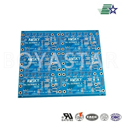
A Gold Finger PCB is designed for plug-in connection applications. It is widely used in memory module cards, graphics card interface boards, industrial control backplanes, and communication equipment plug-in cards that require frequent insertion and extraction connections. Boyastar manufactures Gold Finger PCBs using electroplated hard gold on the gold finger areas. Bevel angle and dimension accuracy are strictly controlled to industry standards. This ensures smooth insertion and reliable contact. We have 18 years of PCB manufacturing experience. We hold IATF 16949 and three other international certifications. Our factory covers 19,000 square meters with over 150 employees. Monthly production capacity reaches 50,000 square meters.
Gold Finger Technology for Reliable Insertion
Gold fingers enable reliable plug-in connections. Our Gold Finger PCB uses electroplated hard gold in the insertion connection areas. Gold thickness is customized based on your insertion cycle requirements, typically from 0.38 μm to 1.27 μm. Bevel angle and dimension accuracy are strictly controlled to industry standards. This ensures smooth insertion and reliable contact. Gold finger areas use electroplated hard gold. Regular circuit areas can use ENIG, HASL, OSP, or other finishes based on your requirements. Impedance tolerance is controlled at ±10% or as per file. This ensures signal integrity during card connection. Layer count ranges from 2 to 20 layers. Board thickness ranges from 0.5 to 3.5 mm or as per your file. All products comply with RoHS and REACH standards and meet UL94 V-0 flame retardant rating.
Precision Gold Finger Manufacturing
Boyastar has mature production technology in gold finger PCB manufacturing. We use dedicated gold finger beveling equipment and AOI automatic optical inspection. Every batch undergoes strict incoming inspection and process control. Gold finger areas receive additional gold thickness testing, hardness testing, and insertion durability sampling. We respond to quality issues within 24 hours. Sample fees are fully deductible from your mass production order. We hold IATF 16949, ISO 9001, ISO 14001, and ISO 45001 certifications. We also hold UL certification with file number E528398. UL certification covers flammability, electrical insulation, and thermal aging tests. These certifications cover quality, environment, occupational health and safety, and product safety. They meet export requirements for North American, EU, and other major markets. Boyastar is your trusted Gold Finger PCB supplier.
Hot Tags: gold finger PCB, China gold finger PCB manufacturers, suppliers, factory, ENIG PCB, Hard Gold Plated PCB, Immersion Silver PCB, Immersion Tin PCB, Lead Free HASL PCB, surface finish pcb
You Might Also Like


Send Inquiry