




Design line width and spacing standards for technical PCB boards
Aug 20, 2026
Leave a message
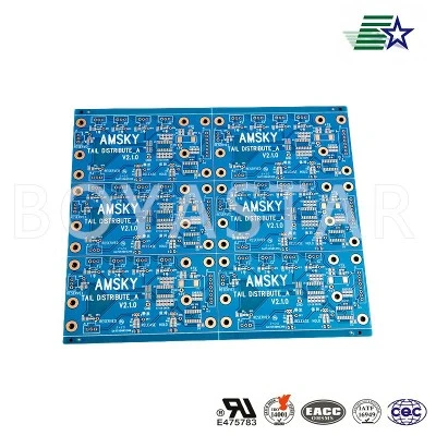
The basic line width and spacing design of technical PCB boards must strictly follow the IPC-2221 industry standard design specifications, while setting benchmark parameters based on the factory's conventional process capabilities, taking into account production yield and design practicality. The general safety standard for ordinary civilian and industrial signal lines in the industry is that the line width and spacing should not be less than 0.15mm (6mil). This parameter is suitable for the production of the vast majority of double-layer and four layer ordinary technical boards, with controllable tolerances and less prone to process defects such as wire breakage and tin connection. The minimum allowable line width and spacing for conventional precision process boards is 0.10mm (4mil), which is only suitable for high-density wiring scenarios; High precision sheet metal relies on high-precision processes to achieve a maximum line width and spacing design of 0.05mm (2mil), but requires exclusive production processes and strict quality control. In daily R&D design, it is recommended to use conservative parameters for non special requirements to avoid the increase of batch production defect rate caused by extreme dimensions.
The line width design of current carrying lines has clear working condition matching standards, and the core is customized based on copper foil thickness, working current, and temperature rise requirements. Under normal temperature conditions, the mainstream 1OZ copper foil sheet in the industry is suitable for low current signal circuits with a line width of over 0.2mm for 100mA, and a line width of not less than 0.4mm for 500mA current circuits. The standard line width for conventional 1A power supply lines is set at 0.6mm or more, and for 2A high current lines, it needs to be widened to 1.0mm or more. For 5A and above high power circuits, it is recommended to use large-area copper laying or multiple parallel wiring designs. Thick copper sheets can be appropriately reduced in line width size, and sufficient safety margins should be reserved during design to avoid high temperature rise and circuit aging and melting problems caused by long-term full load operation of the circuit. At the same time, the distance between power supply lines should be slightly larger than that of ordinary signal lines to prevent electromagnetic coupling interference under high current operation and ensure stable power supply of the circuit.
The design of line spacing in high-voltage insulation areas is the core point of safety regulations, and it is necessary to strictly distinguish the standard of inner and outer layer spacing according to the voltage level. Low voltage signal circuits, conventional 5V, 12V, 24V control circuits, and a safe line distance of 0.15mm between lines can meet insulation requirements; Under the normal voltage condition of AC 220V, the minimum line spacing of the inner layer circuit should not be less than 0.2mm, and the line spacing of the exposed outer layer circuit should be increased to 1.25mm or more. In high-altitude uncoated scenarios, the spacing should be further widened. For high voltage conditions of 380V and above, it is necessary to increase the creepage distance and electrical clearance according to standards, and strictly control the boundary line distance between high and low voltage zones in a graded manner. In addition, the spacing between the circuit, solder pads, and vias should also follow unified standards to eliminate the hidden dangers of arcing, leakage, and short circuits caused by small local spacing, and fully adapt to the safety use standards of various technical PCBs such as industrial control, equipment power supply, and precision electronic control.

Send Inquiry