




Preparation method of technical PCB board
Aug 18, 2026
Leave a message
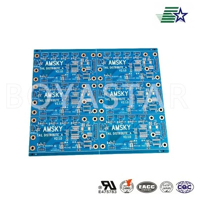
The preliminary process of preparing technical PCB boards mainly revolves around substrate processing and circuit forming, which is the fundamental link to ensure circuit accuracy. In the early stage of production, FR-4, metal substrates and other sheet materials will be cut and trimmed according to the specifications of the board, and the edge dimensions of the board will be adjusted to ensure that the board specifications meet the design drawing standards. Subsequently, moisture and surface impurities inside the board are removed through drying and dust removal to avoid problems such as foaming and poor adhesion in subsequent processes. After the preprocessing is completed, the photosensitive dry film is used to adhere to the surface of the board. The designed circuit pattern is accurately transferred to the surface of the board through exposure and development processes. Then, excess copper foil is removed through etching processes, leaving precise conductive lines and forming a complete circuit framework. The line width and spacing are strictly controlled throughout the process to prevent process defects such as incomplete lines and short circuits.
Middle layer lamination and drilling electroplating are the core key processes in multi-layer, high-precision PCB preparation, which directly determine the structure and electrical performance of the board. For double-layer and multi-layer PCBs, it is necessary to design according to the stacked structure, accurately align and stack the conductive layer and insulation layer, and use high-temperature and high-pressure equipment to press and cure to ensure tight interlayer adhesion and no void delamination. Subsequently, mechanical drilling or laser drilling is carried out according to the positioning standards of the drawings, and conductive holes, positioning holes, and heat dissipation holes are processed. The hole positioning accuracy is strictly adapted to the assembly and conductivity requirements. After the drilling is completed, the hole wall will be polished and the adhesive residue will be removed. Then, a uniform copper layer will be deposited on the hole wall through copper deposition and electroplating processes to achieve stable conductivity of the upper and lower circuits and each layer of circuits. At the same time, the structural strength of the hole wall will be strengthened to prevent problems such as broken holes and poor conductivity during later use.
Surface treatment and post-processing of finished products are important processes for the final preparation of technical PCBs and ensuring their stability during use. After the processing of the circuit and hole positions is completed, the board surface will be subjected to solder mask printing and curing treatment, and uniformly covered with solder mask ink in non-conductive areas to achieve insulation, moisture resistance, oxidation resistance, and short circuit prevention. Subsequently, surface processing is completed according to product requirements. Conventional boards use tin spraying technology, while precision technology PCBs use high-end processes such as immersion gold and gold plating to improve solder joint solderability and oxidation resistance. Finally, silk screen characters, shape edges, chamfering and polishing are carried out to correct defects in the board's appearance. Through processes such as on/off testing, insulation testing, and full appearance inspection, defective products are eliminated to complete the complete preparation of the technical PCB board, ensuring that the finished product is compatible with various precision equipment

Send Inquiry