




Sensor PCB Specifications
Jul 06, 2026
Leave a message
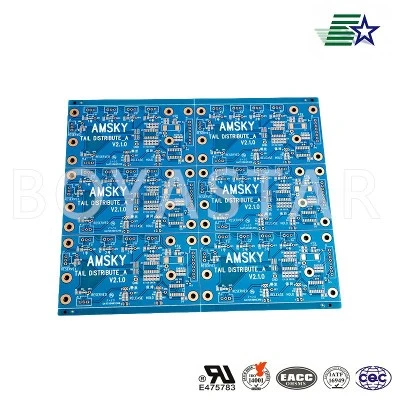
The specifications for sensor PCBs primarily encompass parameters such as board dimensions, thickness, layer count, copper foil thickness, trace width, and trace spacing. Board dimensions are typically determined by the internal mounting space of the sensor device, aiming to minimize the overall footprint while satisfying circuit layout requirements. Board thickness is selected based on product structure and operational needs; insufficient thickness may compromise mechanical strength, whereas excessive thickness adds weight and occupies more space. Consequently, a balanced design approach is required, taking actual installation conditions into account.
Regarding circuit structure, sensor PCBs can be designed as single-layer, double-layer, or multi-layer boards. Devices with simple structures and fewer components often utilize single- or double-layer PCBs, whereas products with complex functionality and circuitry may employ multi-layer boards to provide more routing space and enhance signal transmission performance. Copper foil thickness and trace width are determined by the circuit's operating current; high-current paths generally require wider traces or thicker copper foil to minimize heat generation and voltage loss.
Sensor PCB specifications must also address requirements such as operating voltage, current, temperature range, and mounting method. High-precision sensors necessitate attention to parameters like trace impedance, signal interference, and grounding schemes, while industrial and outdoor equipment requires features such as dust resistance, waterproofing, and tolerance to temperature extremes. Ultimately, PCB specifications are not static; they must be tailored to the specific sensor type, device structure, operating environment, and functional requirements to ensure seamless integration with the overall sensor system.
Send Inquiry