






Wearable Device PCB
A smart watch has very little internal space. The board must be thin, small, and carry high-density routing. We own more than 25 patents. We add 5 to 10 new process patents each year. Our factory is in Guangde Economic Development Zone, Anhui, China. The plant covers 19,000 square meters. We have more than 150 employees. We produce about 50,000 square meters of PCB each month.
Send Inquiry
Thin and Dense for Small Spaces
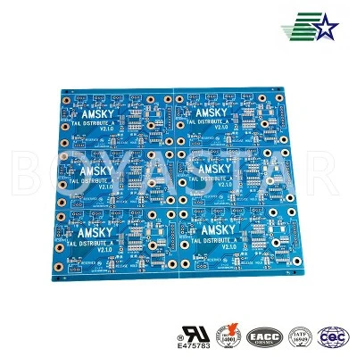
A smart watch has very little internal space. The board must be thin, small, and carry high-density routing. We own more than 25 patents. We add 5 to 10 new process patents each year. Our factory is in Guangde Economic Development Zone, Anhui, China. The plant covers 19,000 square meters. We have more than 150 employees. We produce about 50,000 square meters of PCB each month. The Wearable Device PCB service is a representative product of our high-density interconnect process. This board fits smart watches, smart bands, wireless earphones, VR glasses, and AR glasses. Health monitoring devices, sports tracking devices, and smart clothing also use it. We use FR-4 as the base material. High-density interconnect, blind and buried vias, and BGA are all available. Thin and light design is a key feature. Thin boards, low-power boards, and high-density boards are all within our experience.

Thin Design and Material Options
Layer count ranges from 2 to 10 based on thin design needs. High TG FR-4 and high CTI FR-4 are available. Impedance control is also supported. Surface finishes depend on the project. Immersion gold, HASL, and OSP are common. Immersion silver, immersion tin, and hard gold plating are also supported. Our engineering team has more than ten engineers. They do thin design review and manufacturability analysis. They check the files on the same day. They send a quote and lead time within 24 hours. We accept OEM and ODM orders. We build from drawings. Layer count, board thickness, copper thickness, base material, surface finish, solder mask color, silkscreen color, impedance, blind and buried vias, BGA, and packing all follow the project. Wearable boards must be thin. We use blind and buried vias and high-density interconnect processes. This increases routing density and reduces board thickness to the buyer's target range.

Strength Tests and Full Records
Thin boards can break easily. We run mechanical strength tests, bend tests, and impedance tests. We confirm the first article before release. We keep records for every batch from incoming material to final shipment. Our quality team has more than 20 people. Every board gets 100% electrical testing before packing. We use AOI optical inspection and flying probe testing. We accept third-party inspection. Our factory holds IATF16949, ISO9001, ISO14001, and ISO45001. We hold Underwriters Laboratories product safety certification. The file number is E528398. The Wearable Device PCB service gives buyers a reliable path for thin and dense designs.

Specifications Buyers Need to Know
|
Parameter |
Content |
|
Product Type |
Wearable device PCB for smart watches, bands, wireless earphones, VR/AR glasses |
|
Base Material and Layers |
FR-4, high TG FR-4, high CTI FR-4; supports 2 to 10 layers |
|
Key Processes |
High-density interconnect, blind and buried vias, BGA, thin design, impedance control |
|
Surface Finish |
Immersion gold, HASL, OSP, immersion silver, immersion tin, hard gold plating optional |
|
Engineering Support |
Thin design review and manufacturability analysis |
Hot Tags: wearable device pcb, China wearable device pcb manufacturers, suppliers, factory
Previous:Home Appliance PCB
You Might Also Like


Send Inquiry