





Eco-friendly Concepts for Sensor PCBs
Aug 09, 2026
Leave a message
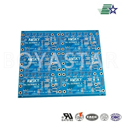
The eco-friendly philosophy behind sensor PCBs is reflected in various stages, including material selection, manufacturing, and usage and maintenance. During the design phase, priority should be given to substrate materials and electronic components that meet environmental standards, thereby minimizing the use of hazardous substances. Furthermore, the PCB's dimensions and circuit layout should be optimized based on the product's actual functionality to avoid material overuse and reduce resource waste during production while still meeting performance requirements.
Attention must be paid to energy consumption and pollutant emissions during manufacturing. PCB production involves processes such as circuit patterning, soldering, and surface finishing; consequently, waste, wastewater, and other pollutants generated during these stages require proper management. Environmental impact can be mitigated by optimizing manufacturing processes, improving material utilization rates, and adopting greener production methods. Additionally, sorting and processing metal offcuts and recyclable materials generated during production helps enhance resource efficiency.
Eco-friendly sensor PCB design also requires consideration of the product's service life. Selecting materials with stable performance, high heat resistance, and reliability reduces the likelihood of malfunctions and the need for frequent replacements, thereby lowering the volume of electronic waste. For long-term sensor equipment, modular design and maintenance-friendly structures allow for the replacement of specific faulty components rather than discarding the entire device; this approach saves costs and reduces electronic waste generation.
Finally, the recycling and disposal of PCBs must be considered once the product reaches the end of its service life. PCBs contain valuable materials such as copper; disposing of them as ordinary waste not only wastes resources but may also harm the environment. Therefore, product design should facilitate disassembly, sorting, and recycling, and spent PCBs should be processed in compliance with environmental regulations. Implementing eco-friendly management across the entire lifecycle-from design and production to usage and end-of-life recycling-minimizes resource consumption and environmental impact while ensuring the sensor PCB's performance.
Send Inquiry